
Electronic and semiconductor manufacturing imposes extremely strict standards on environmental cleanliness and oxygen-free & moisture-free atmosphere. Trace oxygen, water vapor and impurities will trigger wafer oxidation, circuit defects and chip failure, severely reducing product yield. Massive, uninterrupted ultra-high-purity nitrogen is required as shielding gas, purging gas and carrier gas throughout all production processes.
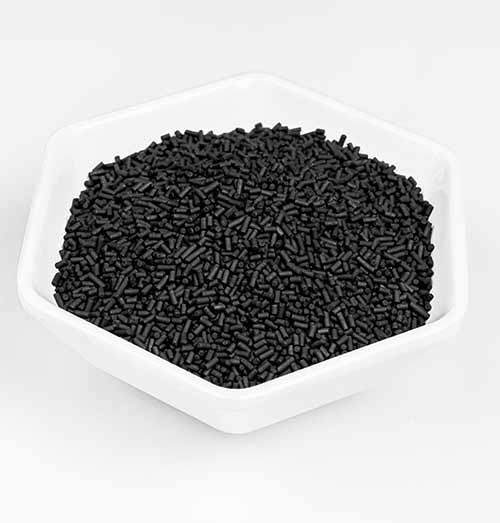
On-site PSA nitrogen generation has become the mainstream gas supply solution for wafer fabs and packaging plants. Carbon Molecular Sieve (CMS) acts as the core adsorbent enabling precise nitrogen-oxygen separation and stable production of 6N ultra-high-purity nitrogen. This article elaborates on the unique functions, application scenarios, exclusive industry advantages and selection criteria of CMS tailored to semiconductor manufacturing demands.
1.Why Ultra-High-Purity Nitrogen Is Mandatory for Semiconductor Production
Trace oxygen and moisture in air cause irreversible damage to precision semiconductor processes:
Nitrogen is chemically inert and dry, isolating air to form a contamination-free production environment. Advanced semiconductor processes demand nitrogen purity of above 99.999% (5N and higher). Ordinary gas separation materials cannot maintain such high purity stably, only high-grade special CMS meets the strict threshold.
2.Core Application Scenarios of CMS PSA Nitrogen in Semiconductor Industrial Chain
2.1 Front-End Wafer Fabrication
2.2 Packaging & Testing
2.3 Auxiliary Plant Scenarios
3.Unique Advantages of CMS PSA Nitrogen for Semiconductor Scenarios
3.1 Stable ultra-high purity output
Semiconductor-grade CMS with sub-angstrom precise pore control delivers outstanding oxygen separation selectivity. Nitrogen purity fluctuation remains minimal during long-term operation, consistently meeting 5N/6N standards for advanced processes and lowering wafer scrap rates.
3.2 Long-cycle stable performance for non-stop production
The material resists acid, alkali and high temperature, maintaining stable adsorption-desorption cycles even with trace corrosive impurities in compressed air. Its service life reaches 8–10 years, minimizing production shutdown losses caused by frequent material replacement.
3.3 Low dust generation to fit cleanroom standards
High mechanical strength and low-dust formulation avoid fine carbon powder release during adsorption, preventing particle contamination of wafers and precision equipment to meet Class 100/1000 cleanroom specifications.
3.4 Energy-saving & low-carbon operation
Room-temperature pressure swing adsorption consumes far less energy than cryogenic separation. Low power consumption per cubic meter of nitrogen reduces electricity expenditure for large wafer fabs and supports low-carbon electronic manufacturing.
4.How CMS Quality Impacts Semiconductor Yield & Operation Costs
Semiconductor processes have an extremely low tolerance for gas impurities. CMS performance directly determines chip yield and equipment maintenance costs:
4.1 Superior Performance of Semiconductor-Grade High-Quality CMS
4.2 Production Losses Caused by Inferior CMS
5.CMS Selection Standards Tailored for Electronics & Semiconductor Industry
Wafer fabs and packaging plants shall focus on industry-specific indicators during CMS procurement:
Professional CMS suppliers can customize adsorbents for logic chips, memory chips, advanced packaging and panel manufacturing, balancing nitrogen production efficiency, purity and long-term comprehensive operating costs.
6.Conclusion
Ultra-high-purity nitrogen serves as the fundamental process gas covering wafer fabrication, packaging and testing in the semiconductor industry. As the core functional material of on-site PSA nitrogen generators, CMS enables low-cost, stable and continuous supply of ultra-high-purity nitrogen.
Premium semiconductor-specific CMS not only steadily delivers 5N~6N nitrogen to eliminate process defects induced by oxygen and moisture and boost chip yield, but also features low energy consumption, low dust and long service life to reduce overall factory expenditure on gas supply and equipment maintenance.
Whether for advanced lithography, thin-film deposition and ion implantation in front-end processes, or SMT soldering and chip packaging in back-end stages, selecting high-performance CMS matched to working conditions is a critical investment for electronic and semiconductor enterprises to guarantee product quality and realize stable mass production.
يرجى مواصلة القراءة، والبقاء على اطلاع، والاشتراك، ونحن نرحب بك لتخبرنا بما تفكر فيه.

حقوق الطبع والنشر
@ 2026 شركة تشيتشو شانلي للمنخل الجزيئي المحدودة جميع الحقوق محفوظة.
 الشبكة المدعومة
Hi! Click one of our members below to chat on